| 4A B Building Zhuao Industrial Park Gushu Xixiang Baoan District Shenzhen,China,518126 | info@newbridge.com.cn |
| 4A B Building Zhuao Industrial Park Gushu Xixiang Baoan District Shenzhen,China,518126 | info@newbridge.com.cn |
 |
| Place of Origin: | SHENZHEN,CHINA |
| Brand Name: | NEWBRIDGE |
| Certification: | FCC,CE |
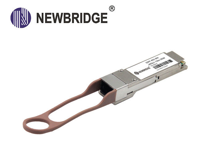
| Model Number: | NDQP-40G-SR4 |
| Minimum Order Quantity: | 1PC |
|---|---|
| Price: | Negotiation |
| Packaging Details: | packing can be done by customer's requested, usually used in carton |
| Delivery Time: | According to the quantiy and stocking , 3-4 working days after payment |
| Payment Terms: | T/T , Western Union |
| Supply Ability: | According to the different products , the monthly output is different |
| Fiber: | Single Fiber | Device Type: | Optical SFP Module |
|---|---|---|---|
| Data Rate: | 40G | Operating Temperature: | 0°C To 70°C |
| Power Supply: | +3.3V | Low Power Consumptionor: | <1W |
NDQP-40G-SR4 40G QSFP+ optical transceiver is designed according to QSFP Multi-Source Agreement (MSA) and compliant with 40GBASE-SR4 of the IEEE P802.3ba standard. It supports the reach of 100m on OM3 fiber and 150m on OM4 fiber.
² Up to 11.2Gbps per channel bandwidth
² Aggregate bandwidth up to 40Gbps
² Hot-pluggable
² MPO-12 connector
² Up to 100m on OM3 and 150m on OM4
² Compliant with 40G Ethernet IEEE802.3ba
² QSFP MSA compliant
² Built-in digital diagnostic functions
² Power Supply :+3.3V
² Power consumption: <1.5W
² Temperature Range: 0~ 70°C
² RoHS Compliant
² 40GBASE Ethernet
² InfiniBand QDR, DDR and SDR
| Part Number | Data Rate | Distance | Wavelength | Fiber | DDM | Connector |
| NDQP-40G-SR4 | 40Gb/s | 150m | 850nm | MMF | Yes | MPO-12 |
Absolute Maximum Ratings
| Parameter | Symbol | Min. | Typical | Max. | Unit |
| Storage Temperature | TS | -40 | +85 | °C | |
| Supply Voltage | VCCT, R | -0.5 | 4 | V | |
| Relative Humidity | RH | 0 | 85 | % |
Recommended Operating Environment:
| Parameter | Symbol | Min. | Typical | Max. | Unit |
| Case operating Temperature | TC | 0 | +70 | °C | |
| Supply Voltage | VCCT, R | +3.135 | +3.465 | V | |
| Supply Current | ICC | 475 | mA | ||
| Power Dissipation | PD | 1.5 | W |
Electrical Characteristics (TOP = 0 to 70 °C, VCC = 3.135 to 3.465 Volts)
| Parameter | Symbol | Min | Typ | Max | Unit | Note | |
| Transmitter | |||||||
| Single Ended Output Voltage Tolerance | 0.3 | 4 | V | 1 | |||
| Common mode Voltage Tolerance | 15 | mV | |||||
| Transmit Input Diff Impedance | ZIN | 85 | 100 | 115 | |||
| TX Disable | Disable | VIH | 2 | VCC+0.3 | |||
| Enable | VIL | 0 | 0.8 | ||||
| TX Fault | Fault | VOH | 2.4 | VCC+0.3 | |||
| Normal | VOL | 0 | 0.5 | ||||
| Receiver | |||||||
| Single Ended Output Voltage Tolerance | -0.3 | 4 | V | ||||
| AC common mode voltage | 7.5 | mV | |||||
| Termination mismatch at 1MHz | 5 | % | |||||
| Output Impedance (Differential) | Zout | 85 | 100 | 115 | ohms | ||
| Output Rise/Fall Time | tr /tf | 30 | ps | 10%~90% | |||
| RX_LOS | LOS | VOH | 2.4 | VCC+0.3 | V | ||
| Normal | VOL | 0 | 0.8 | V | |||
| Parameter | Symbol | Min | Typ | Max | Unit | Ref. | ||
| Transmitter | ||||||||
| Central Wavelength | λ0 | 840 | 850 | 860 | nm | |||
| RMS spectral width | RMS | 0.65 | nm | |||||
| Average Launch Power, each Lane | Po | -7.6 | - | +2.4 | dBm | |||
| Optical Modulation Amplitude, each Lane | OMA | -5.6 | 3 | dBm | ||||
| Difference in launch power between any two lanes(OMA) | 4 | dB | ||||||
| TDP, each Lane | TDP | 3.5 | dB | |||||
| Extinction Ratio | ER | 3 | dB | 2 | ||||
| Optical Return Loss Tolerance | 12 | dB | ||||||
| Average launch power of OFF, each lane | -30 | dBm | ||||||
| Output Optical Eye | IEEE 802.3ba-2010 Compliant | 2 | ||||||
| TX Disable Assert Time | t_off | 100 | μs | |||||
| Receiver | ||||||||
| Central Wavelength | λc | 840 | 850 | 860 | nm | |||
| Stressed receiver sensitivity in OMA, each lane | Pmins | -5.4 | dBm | |||||
| Maximum Receive Power, each lane | Pmax | 2.4 | dBm | |||||
| Average power, each lane | Rx | -7.0 | 1.0 | dBm | 3 | |||
| Damage Threshold | 3.4 | dBm | ||||||
| Receiver reflectance | Rr | -12 | dB | |||||
| LOS De-Assert | LOSD | -7.5 | dBm | |||||
| LOS Assert | LOSA | -30 | dBm | |||||
| LOS Hysteresis | LOSH | 0.5 | dB | |||||
Pin Function Definitions
| Pin | Logic | Symbol | Name/Description | Note |
| 1 | GND | Ground | 1 | |
| 2 | CML-I | Tx2n | Transmitter Inverted Data Input | |
| 3 | CML-I | Tx2p | Transmitter Non-Inverted Data output | |
| 4 | GND | Ground | 1 | |
| 5 | CML-I | Tx4n | Transmitter Inverted Data Output | |
| 6 | CML-I | Tx4p | Transmitter Non-Inverted Data Output | |
| 7 | GND | Ground | 1 | |
| 8 | LVTTL-I | ModSelL | Module Select | |
| 9 | LVTTL-I | ResetL | Module Reset | |
| 10 | VccRx | +3.3V Power Supply Receiver | 2 | |
| 11 | LVCMOS-I/O | SCL | 2-Wire Serial Interface Clock | |
| 12 | LVCMOS-I/O | SDA | 2-Wire Serial Interface Data | |
| 13 | GND | Ground | 1 | |
| 14 | CML-O | Rx3p | Receiver Inverted Data Output | |
| 15 | CML-O | Rx3n | Receiver Non-Inverted Data Output | |
| 16 | GND | Ground | 1 | |
| 17 | CML-O | Rx1p | Receiver Inverted Data Output | |
| 18 | CML-O | Rx1n | Receiver Non-Inverted Data Output | |
| 19 | GND | Ground | 1 | |
| 20 | GND | Ground | 1 | |
| 21 | CML-O | Rx2n | Receiver Inverted Data Output | |
| 22 | CML-O | Rx2p | Receiver Non-Inverted Data Output | |
| 23 | GND | Ground | 1 | |
| 24 | CML-O | Rx4n | Receiver Inverted Data Output | |
| 25 | CML-O | Rx4p | Receiver Non-Inverted Data Output | |
| 26 | GND | Ground | 1 | |
| 27 | LVTTL-O | ModPrsL | Module Present | |
| 28 | LVTTL-O | IntL | Interrupt | |
| 29 | VccTx | +3.3V Power Supply Transmitter | 2 | |
| 30 | Vcc1 | +3.3V Power Supply | 2 | |
| 31 | LVTTL-I | LPMode | Low Power Mode | |
| 32 | GND | Ground | 1 | |
| 33 | CML-I | Tx3p | Transmitter Inverted Data Output | |
| 34 | CML-I | Tx3n | Transmitter Non-Inverted Data Output | |
| 35 | GND | Ground | 1 | |
| 36 | CML-I | Tx1p | Transmitter Inverted Data Output | |
| 37 | CML-I | Tx1n | Transmitter Non-Inverted Data Output | |
| 38 | GND | Ground | 1 |
Digital diagnostics monitoring function is available on all QSFP+ SR4. A 2-wire serial interface provides user to contact with module. The structure of the memory is shown in flowing. The memory space is arranged into a lower, single page, address space of 128 bytes and multiple upper address space pages. This structure permits timely access to addresses in the lower page, such as Interrupt Flags and Monitors. Less time critical time entries, such as serial ID information and threshold settings, are available with the Page Select function. The interface address used is A0xh and is mainly used for time critical data like interrupt handling in order to enable a one-time-read for all data related to an interrupt situation. After an interrupt, IntL, has been asserted, the host can read out the flag field to determine the affected channel and type of flag.
| Address |
Length (Byte) |
Name | Description and Contents |
| Base ID Fields | |||
| 128 | 1 | Identifier | Type of Serial transceiver |
| 129 | 1 | Ext. Identifier | Extended identifier of type serial transceiver ( |
| 130 | 1 | Connector | Code of optical connector type |
| 131~138 | 8 | Transceiver | Code of electronic compatibility or optical compatibility |
| 139 | 1 | Encoding | 64B/66B |
| 140 | 1 | BR, Nominal | Nominal baud rate, unit of 100Mbps |
| 141 | 1 | Extended rate select compliance | Tags for extended rate select compliance |
| 142 | 1 | Length(9μm) | Link length supported for 9/125μm fiber, units of km |
| 143 | 1 | Length(E-50μm) | Link length supported for EBW 50/125μm fiber, units of 2m |
| 144 | 1 | Length(50μm) | Link length supported for 50/125μm fiber, units of meters |
| 145 | 1 | Length(62.5μm) | Link length supported for 62.5/125μm fiber, units of meters |
| 146 | 1 | Length(Copper) | Link length supported for copper, units of meters |
| 147 | 1 | Device tech | Device technology |
| 148~163 | 16 | Vendor Name | QSFP+ vendor name (ASCII) |
| 164 | 1 | Extended transceiver | Extended transceiver codes for infiniBand |
| 165~167 | 3 | Vendor OUI | QSFP transceiver vendor OUI ID (ASCII) |
| 168~183 | 16 | Vendor PN | Part Number (ASCII) |
| 184~185 | 2 | Vendor rev | Revision level for part Number (ASCII) |
| 186~187 | 2 | Wavelength | Nominal laser wavelength (value / 20 in nm) |
| 188~189 | 2 | Wavelength tolerance | Guaranteed rage of laser wavelength (+/- value) from nominal wavelength (value/200 in nm) |
| 190 | 1 | Max. case temp. | Maximum case temperatures in degree C |
| 191 | 1 | CC-BASE | Check code for base ID fields (addresses 128~190) |
| Extended ID Field | |||
| 192~195 | 4 | Options | Rate select, TX disable, TX fault, LOS |
| 196~211 | 16 | Vendor SN | Serial Number (ASCII) |
| 212~219 | 8 | Date code | Manufacturing date code |
| 220 | 1 | Diagnostic monitoring type | Type of diagnostic monitoring implemented |
| 221 | 1 | Enhanced options | Optional enhanced features that are implemented |
| 222 | 1 | Reserved | Reserved |
| 223 | 1 | CC-EXT | Check code for the extended ID Fields (addresses 192~222) |
| Vendor Specific ID Field | |||
| 224~255 | 32 | Vendor specific | Vendor specific EEPROM |
SD HD SDI Converter , 20km 40km 60km Optional Mini Converter with single mode or single fiber
DC 12V Hdmi To Hd Sdi Converter SDI Signal Loop Out With 158×120×36mm Size
5V~24VDC Hdmi To Hd Sdi Converter 720p/1080p With 2 Channel SDI Signal Out
Plug And Play 60km HD SDI Converter , SD Auto Detection Optical Transceiver
RJ45 Port 100M Industrial Ethernet Switch/8 PoE port industrial network switch
High Efficiency 8 Port SFP PoE Ethernet Switch High Efficiency Easy Operating
Full Duplex Operation 24 Port PoE Ethernet Switch RJ45 Ports 100m 8.8G
LCD Display 16 Port Ethernet Switch 10 100Mbps 2G TP / SFP AC 240V Accurate
3D Video 4K HD HDMI Splitter 1 x 8 HDMI Splitter 1 In 8 Out
4K 1.4b 1 x 4 HDMI Splitter 1 In 4 Out Supporting 3D Video CE Certification
100Mbps RJ45 DC output 12V port poe splitter support IEEE 802.3at Poe Splitter HD HDMI Splitter